
No modern society without semiconductor chips
Hi there, Håkan Pettersson, professor of physics with a focus on semiconductor physics at Halmstad University. You are part of a large research group specialising in semiconductors and nanotechnology. Can you tell us more about why this research is so important?
“‘There is no digital without chips’, president of the European Commission, Ursula von der Leyen, stated as she introduced the European Chips Act in 2022. In other words, we would not have a modern society without semiconductor chips.
Access to semiconductor technology is not only the basis for the digital transformation of our modern society but also required for three important areas: the green transition with chip power reduction to avoid excessive energy consumption, the electrification with efficient power handling, and future AI systems where dedicated chips are required for quantum technologies and brain-inspired computing.”

Semiconductors are at the heart of technological innovation and absolutely crucial to both current and tomorrow’s modern information society.
Can you describe recent developments in your research?
“We are deeply engaged in the recently launched long-term Vinnova Excellence Centre ‘Advanced Chip Technologies (ACT)’, coordinated by Lund University. In this consortium, we are developing three generic key digital technologies: high-speed electronics, optoelectronics and power electronics. These are base technologies already used in Swedish industry and well supported by academic research. We will continue to work on these existing technologies to support industry, but more importantly, we will develop strategies for disruptive heterogeneous 3D integration of device layers on commercial silicon platforms.
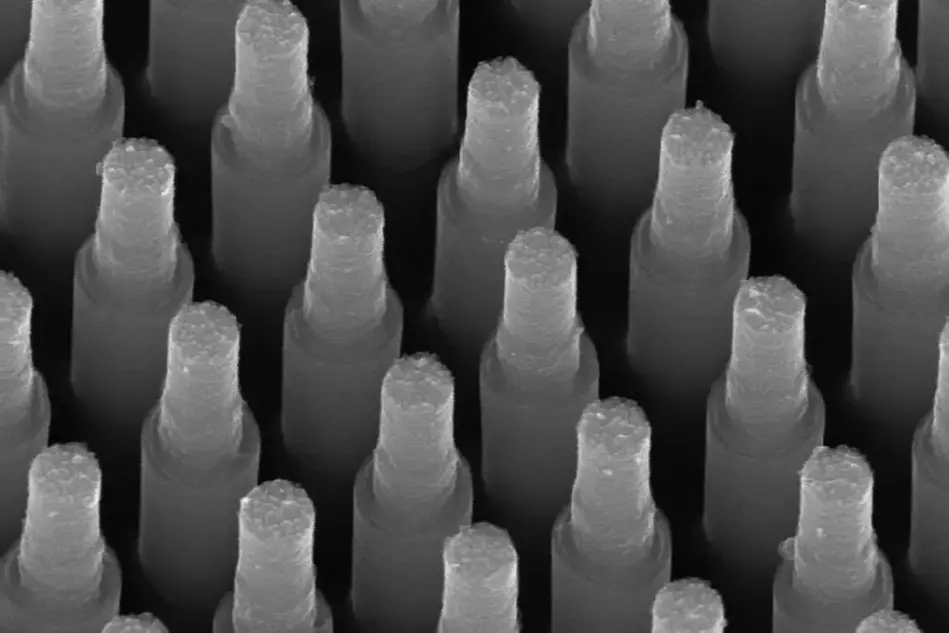
Nanowires, magnified 130.000 times.
Recently, we have recruited a new PhD student, Surya Prakash, to ACT. He will develop advanced optical sensors based on nanowires, which are needle-like semiconductor crystals about one thousand times thinner than a strand of hair. These sensors are unique in that different semiconductors can be combined along each nanowire, which makes it possible to selectively detect a specific portion of infrared radiation. This is of key importance for, for example, advanced surveillance through clouds, smoke and haze with applications in defence, security, agriculture and the environment. The nanowires also have a unique built-in gain mechanism, which provides a very high sensitivity. The project is carried out together with Lund University, the Royal Institute of Technology (KTH) and the Swedish detector manufacturing company IRnova.”
The semiconductor research group in Halmstad has also recently obtained a renewed four-year grant from the Swedish Research Council (VR). What will this funding be used for?
“Our project is primarily about in-depth studies of the physical origin and implementation of a complex interaction between infrared radiation and peculiar defects on the surfaces of nanowires discovered in our previous VR grant. This hitherto unknown mechanism facilitates the development of different types of optical sensors with tailored performance targeting extremely high sensitivity – down to the detection of single light particles, so-called photons. Another application area is optoelectronic synapses and artificial retinas where the individual nanowires ‘remember’ previously incoming light pulses mimicking biological synapses in the human brain. For this project we have recruited another new PhD student, Arzoo Kathewadi.”
For the past few months, you have been part of Semicon Sweden, a new national centre of excellence that focuses on semiconductors. Tell us more!
“Funded by The Swedish Agency for Economic and Regional Growth, Halmstad University was recently granted part of the four-year project Semicon Sweden, together with Svensk Elektronik, Sweden’s foremost trade association for industrial electronics, Lund University, RISE and several industrial partners with the aim of forging a broad alliance to fortify Sweden’s national semiconductor ecosystem.
With this initiative, Sweden is taking the next step to strengthen its position in Europe and establish itself as a significant player in semiconductor technology and future electronics. This initiative aims to create a strong ecosystem for innovation and industrial growth by connecting academia, companies and research institutes. The goal is to increase competitiveness, attract more investments and strengthen Sweden’s role in European collaborations, including the Chips Joint Undertaking, which is a European tripartite partnership boosting the development and adoption of advanced nanoelectronic chip technologies and systems manufactured in Europe.”
Photos: Vinnova Excellence Centre ACT and Håkan Pettersson
What is a semiconductor?
Semiconductors are materials whose electrical conductivity can be precisely controlled in a broad range, from being insulating to highly conductive. They can also efficiently convert electromagnetic radiation, for example sunlight or infrared radiation, to an electric signal. Semiconductors are at the heart of technological innovation and absolutely crucial to both current and tomorrow’s modern information society. They also play a fundamental role in the green and digital transitions.
